

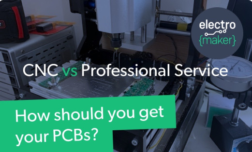
Will AI-Powered Cloud Native PCB Routing Make Traditional Auto-Routers Obsolete?
As technology advances, the importance of efficient and accurate PCB routing cannot be overstated. Traditional auto-routers have long been a source of frustration for engineers, often producing subpar results and requiring significant manual intervention. The introduction of AI into this space promises to transform the way PCBs are designed and manufactured, making the process faster and more reliable.
Nabil explains how Deep PCB's unique approach to PCB routing leverages AI and machine learning to overcome traditional methods' limitations. We'll delve into their technology, the challenges they address, and their solutions' industry impact.
Overview of Deep PCB AI-Powered Cloud Native PCB Routing
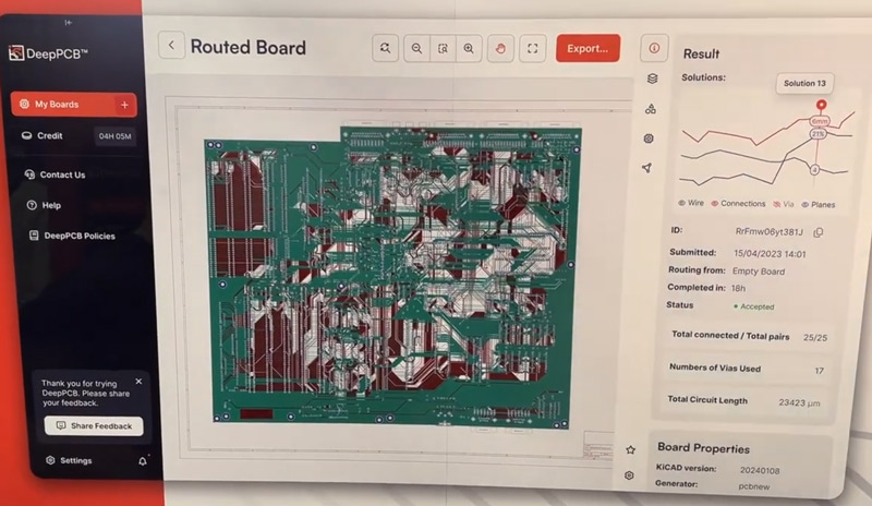
DeepPCB leads innovation in PCB design with its cloud-native AI-powered solution. It excels in performing complex routing and placement tasks that typically require extensive manual effort and expertise.
Traditional auto-routers struggle with complex designs, especially with multiple layers, differential pairs, and intricate constraints. These systems often produce suboptimal results, necessitating significant manual adjustments.
Deep PCB's AI-powered solution uses advanced machine learning to continuously improve its performance. This approach enhances routing quality and reduces the time and effort required from engineers, allowing them to focus on critical design aspects.
Features and Capabilities
The Portenta carrier board, seamlessly integrates with the Portenta product family, enhancing its functionality and versatility for complex projects.
The Portenta carrier board features:
- GPIO Breakout: Easy access to input/output pins.
- Mini PCI Express: Supports additional peripherals and expansion cards.
- Camera Connector: Facilitates camera module integration.
- Ethernet: Reliable, high-speed network connectivity.
- Additional I/Os: Supports diverse project requirements.
These features make the Portenta carrier board a powerful platform for developers, providing comprehensive tools and connectivity options for high-quality results.
Addressing Challenges in PCB Routing
Traditional PCB routing faces challenges with planes, differential pairs, and constraints. These complexities often lead to suboptimal results and require extensive manual adjustments.
Deep PCB's AI-powered solution leverages reinforcement learning, training through millions of simulations to perform tasks with increasing accuracy. This results in high-quality routing that meets modern PCB design's stringent demands, reducing development time and enabling faster prototyping.
Industry Impact and Applications
Deep PCB's AI-powered technology can significantly impact the PCB design industry by streamlining routing and placement, accelerating the prototyping process, and reducing development cycles.
This technology enhances efficiency in designing complex PCBs, valuable in IoT, automation, and industrial solutions. It automates tedious design aspects, allowing engineers to focus on innovation.
In IoT, efficient and reliable PCB routing is crucial. Deep PCB's solution ensures precision and meets rigorous demands while shortening development timelines.
Automation systems benefit from maintaining signal integrity and optimizing critical paths. In industrial applications, the technology minimizes design flaws, ensuring reliability and continuous operation.
Overall, Deep PCB's AI-powered routing technology is poised to revolutionize the PCB design process, delivering high-quality, efficient routing and placement across various industries.
Real-World Application and User Experience
Deep PCB's technology has significantly impacted various projects, evidenced by user case studies. One electronics manufacturer reduced design time by over 50%, bringing products to market faster. A startup developing IoT devices found the solution handled complex tasks and identified design improvements.
Overall, Deep PCB's AI-powered routing technology revolutionizes the PCB design process, delivering significant benefits to engineers and designers across various industries.
Limitations and Future Developments
Deep PCB's technology has limitations, such as handling RF traces, requiring manual placement and keep-out zones. However, they are working on enhancements, including an AI-driven placement feature to automate the placement process.
The AI placement tool will analyze schematics and extract constraints, offering initial placement suggestions. This speeds up the design process and identifies potential issues early on.
Future developments include enhancing AI learning capabilities with extensive datasets and integrating with more design software tools for a seamless experience.
Despite current limitations, Deep PCB's future developments promise a more powerful tool for PCB designers, streamlining the design process and enabling higher efficiency and precision in projects.


Leave your feedback...